The Union Cabinet approved two new semiconductor projects in Gujarat under India Semiconductor Mission, including India's first GaN-based Mini/Micro-LED display facility, with combined investment of ?3,936 crore and 2,230 jobs expected.
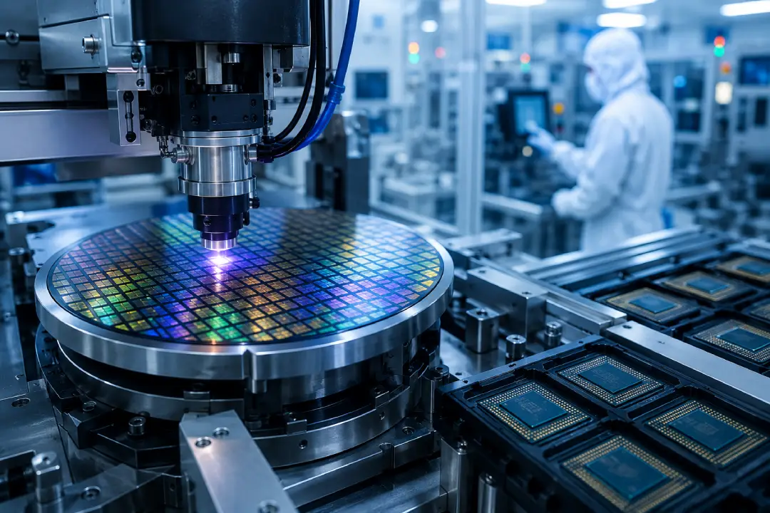
The Union Cabinet, chaired by Prime Minister Narendra Modi, has approved two new semiconductor projects under the India Semiconductor Mission (ISM), marking another significant milestone in the country's drive to build a self-reliant and globally competitive semiconductor ecosystem. Both facilities will be set up in Gujarat, with a combined investment of approximately Rs. 3,936 crore and an expected creation of 2,230 skilled jobs. With these approvals, the total number of projects sanctioned under ISM rises to 12, carrying cumulative investments of around Rs. 1.64 lakh crore.
The two newly approved projects span distinct but complementary segments of the semiconductor value chain — advanced compound semiconductor display manufacturing and outsourced semiconductor assembly and testing — reinforcing India's ambition to develop end-to-end capabilities in one of the world's most strategically important technology sectors.
The first approved project, by Crystal Matrix Limited (CML), will establish an integrated compound semiconductor fabrication and Assembly, Testing, Marking, and Packaging (ATMP) facility at Dholera, Gujarat. This facility will be India's first commercial Mini/Micro-LED display manufacturing plant based on Gallium Nitride (GaN) technology, a material prized for its superior electron mobility, energy efficiency, and high-power performance compared to traditional silicon.
The Dholera facility will also offer GaN foundry services, including epitaxial growth on 6-inch wafers, establishing it as a full-stack compound semiconductor hub. The annual proposed production capacity includes 72,000 square metres of Mini/Micro-LED display panels and 24,000 sets of RGB GaN Epitaxy Wafers. These outputs will serve a wide spectrum of applications — large-format displays for televisions and commercial signage, medium-sized displays for tablets, smartphones, and automotive in-car systems, as well as micro-displays for Extended Reality (XR) glasses and smartwatches.
The approval of this facility is particularly significant as Mini/Micro-LED technology is fast emerging as the successor to conventional LCD and OLED display technologies, offering superior brightness, contrast, and energy efficiency. India's entry into this space at the manufacturing level places the country at the frontier of next-generation display technology.
The second approved project, by Suchi Semicon Private Limited (SSPL), will establish an Outsourced Semiconductor Assembly and Test (OSAT) facility in Surat, Gujarat, focused on the manufacturing of discrete semiconductors. With a proposed production capacity of 1,033.20 million chips per annum, the facility will significantly enhance India's downstream semiconductor packaging capabilities.
The facility's output is targeted at high-demand end markets including power electronics, analog integrated circuits (ICs), and industrial systems. Its customers are expected to span the automotive, industrial automation, and consumer electronics sectors — all of which are experiencing rapid growth in semiconductor content per device. The Surat facility will complement India's upstream chip design strengths with scalable downstream manufacturing, addressing a critical gap in the domestic semiconductor value chain.
Approved Projects: At a Glance
|
Company |
Crystal Matrix Limited (CML) |
|
Location |
Dholera, Gujarat |
|
Technology |
GaN-based Mini/Micro-LED, 6" wafer epitaxy |
|
Capacity |
72,000 sq. m. display panels; 24,000 RGB wafer sets p.a. |
|
Applications |
TVs, tablets, smartphones, in-car displays, XR glasses, smartwatches |
|
Company |
Suchi Semicon Private Limited (SSPL) |
|
Location |
Surat, Gujarat |
|
Technology |
OSAT — discrete semiconductor packaging |
|
Capacity |
1,033.20 million chips per annum |
|
Applications |
Power electronics, analog ICs, automotive, industrial automation |
|
Combined Investment |
Rs. 3,936 crore |
|
Employment Expected |
2,230 skilled professionals |
With these two additions, India's semiconductor pipeline under ISM now comprises 12 approved projects with cumulative investments of approximately Rs. 1.64 lakh crore. The pace of progress is accelerating: of the ten projects approved prior to this announcement, two have already commenced commercial shipments from India, and two more are expected to begin commercial production shortly.
These manufacturing approvals are being reinforced by equally significant investments in chip design capabilities. The government has extended design infrastructure support to 315 academic institutions and 104 start-ups, building a talent pipeline and innovation ecosystem that will underpin India's long-term competitiveness in the global semiconductor industry. Together, these initiatives signal India's transition from a semiconductor importer to an emerging node in the global semiconductor supply chain.
India's entry into compound semiconductor manufacturing — through GaN-based Mini/Micro-LED technology — marks a qualitative leap beyond conventional silicon chip assembly. Compound semiconductors, made from combinations of elements such as Gallium and Nitrogen, enable devices to operate at higher frequencies, higher voltages, and higher temperatures than silicon-based alternatives. They are foundational to 5G communications, electric vehicles, satellite systems, advanced defence electronics, and next-generation displays.
By establishing domestic manufacturing capacity in this segment, India is not merely building an industrial base — it is positioning itself to participate in the high-value, rapidly growing markets of the future. The ISM approvals to date, spanning silicon chip packaging, compound semiconductor fabrication, and advanced display manufacturing, collectively represent a strategic, multi-layered bet on India's capacity to become a trusted global node in the semiconductor supply chain.